

Tutorials
Donut Board: How to Connect Pads and Solder Your Circuit
Aug
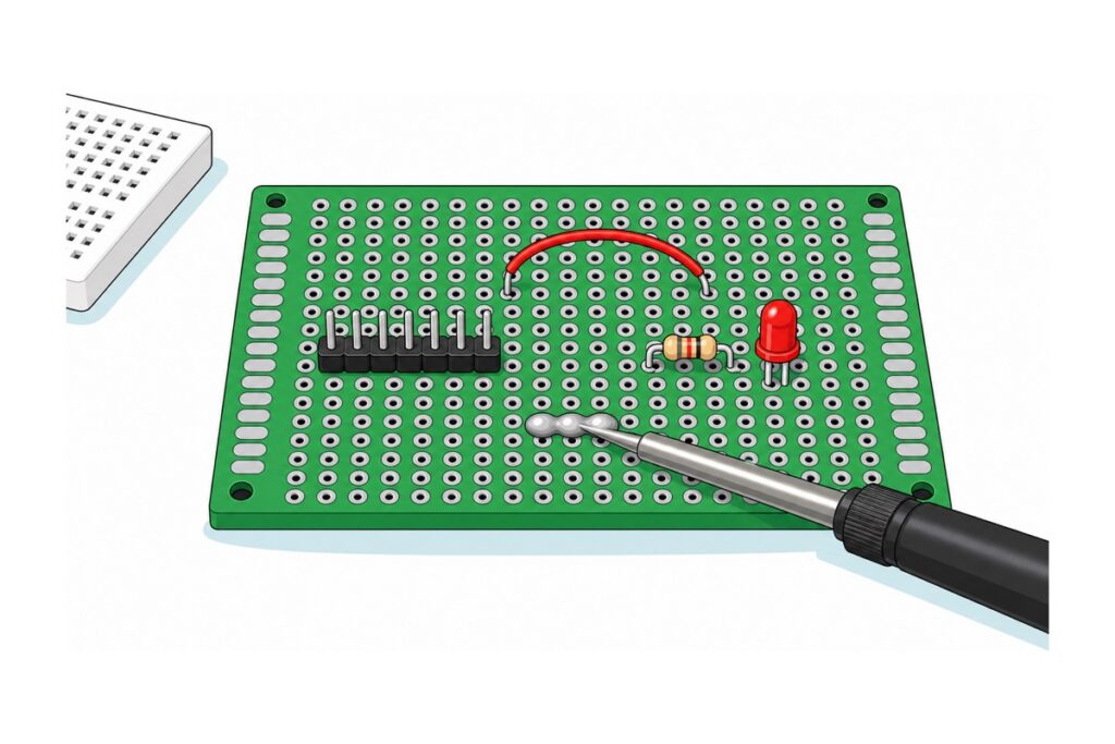
A donut board joins nothing on its own. Every silver ring on it is an electrical island — no hidden rows, no copper strips — so a connection exists only where you make one: a solder bridge across neighbouring pads, an insulated wire, or a bent component leg. That fact separates a working breadboard from a soldered board that is not.
Most people arrive mid-project, the circuit already running: “sekrng nk step kemaskan solder… solder ke board hijau ye tuan”. That green board is this one. Malaysia calls it a donut board, after the ring-shaped pads; elsewhere it sells as perfboard or a prototype PCB.
Why does nothing on a donut board connect to anything?
The donut board is the exact opposite of a breadboard. Its green fibreglass is drilled on a 2.54 mm (0.1 inch) grid — the same pitch as breadboard holes, header pins and DIP chip legs, which is why the transfer works at all. Each hole is ringed by a tinned copper pad — the “donut” — and the fibreglass between two rings insulates them.
“Double sided” does not mean anything is pre-wired. It means each hole carries a pad on the top face and a matching pad underneath, joined by a plated barrel through the hole — one node with two faces, so you solder from whichever is convenient and a leg pushed through reaches both. What it does not buy you is two routing layers: since the two faces of one hole are already the same node, a bridge made underneath joins those pads on the top face too. Crossings are made with insulated wire over the component side, never by swapping faces.
A breadboard hides five holes per row behind a spring clip and runs power rails of twenty-five holes or more; none of that survives the move. Nor is this stripboard — Veroboard carries continuous copper strips you must cut to break connections, and a donut board has none. Every path here is additive.
Sizes follow the same grid — 2.54 mm pitch is just under four holes per centimetre, less an edge margin — and the 2×8 cm strip prints its own coordinates, rows A–F, columns 1–28.
| Board | Size | Roughly | Good for |
|---|---|---|---|
| DNB0208 | 2 × 8 cm | 6 × 28 pads | One sensor or driver, sitting beside something else |
| DNB0406 | 4 × 6 cm | ≈14 × 20 pads | A single circuit block plus a rail |
| DNB0507 | 5 × 7 cm | ≈18 × 24 pads | The classic project size: MCU on sockets, rails, a few modules |
| DNB0709 | 7 × 9 cm | ≈26 × 31 pads | A whole build with gaps left between blocks |
| DNB1218 | 12 × 18 cm | about 3,000 pads | Panels, several boards together, or cut down to size |
Cutting one down is score-and-snap, not a saw job: the hole rows are already a perforation line, so run a sharp craft knife hard along a single row on both faces against a steel rule, then snap the board over a table edge; that row of pads is sacrificed, so count it out of the layout first. Do it before any component goes on, and wipe the dust away rather than blowing it — the board is glass fibre.
Parts list — moving one breadboard circuit onto a donut board
 Double Sided Donut Board DIY Robotics Prototype Board PCB Circuit Board - DONUT BOARD (5CM*7CM)
 50g Soldering Wire Lead with Flux Core 1mm Diameter
 80W Electronics Soldering Iron with LCD Display Ajustable Temperature Microconstroller Electronic Project
 Diagonal Plier Tool Plato Model 170 Removel Tool 3D Module Cutter Trimmer Gundum
 Breadboard Jumper Wire Set Male to Male Bread Board Wire Solderless Connection
Optional — undo it, prove it, work more comfortably
| Item | Price | Qty | |
|---|---|---|---|
 Desoldering Pump Solder Cleaner Sucker Vacuum Soldering RemovalDESOLPU Desoldering Pump Solder Cleaner Sucker Vacuum Soldering RemovalDESOLPU | RM6.95 | ||
 XL830L Digital Multimeter with backlight Portable Multimeter Electronics ProjectMULTIME XL830L Digital Multimeter with backlight Portable Multimeter Electronics ProjectMULTIME | RM25.95 | ||
 Mini Soldering Stand Full Metal Portable Solder Iron Stand with SpongeSSTANDS Mini Soldering Stand Full Metal Portable Solder Iron Stand with SpongeSSTANDS | RM2.20 | ||
 20g Soldering Paste Rosin Flux Lead-Free Blending Easy SolderSOPASTE 20g Soldering Paste Rosin Flux Lead-Free Blending Easy SolderSOPASTE | RM12.95 | Out of stock |
The desoldering pump is the cure for the accidental bridge this guide warns about: heat the joint, hold the nozzle against the molten pool, press the button. The multimeter's continuity beeper is how you prove a joint before the first power-up. The stand keeps a 300 °C barrel somewhere other than your desk, and extra rosin paste helps solder wet an older, duller pad when the flux inside the wire is not enough.
One paragraph of housekeeping before the first joint. The iron is mains powered and its tip sits at a few hundred degrees: work in moving air, park it in its stand every time you let go of it, never touch the barrel to check whether it is hot, and expect flux to spit — the cutter’s own handles carry a safety-glasses warning. The solder is leaded, so wash your hands afterwards and keep food off the bench. Which iron and which flux to buy is a separate subject — see our soldering iron and flux guide, and how to solder header pins for the motion of one clean joint, which is the same motion everywhere on this board.
Where does the ground go when the breadboard rail disappears?
Ground is what actually blocks people, almost verbatim: “banyak sambung yang nak kene sambung pada esp32… mcm ground banyak komponen nak sambung kat kaki ground… so nak kene buat apa ye” — many components needing ground, one GND pin. The breadboard’s side rail solved that silently. A donut board has none until you build one, so build it first, before any component.
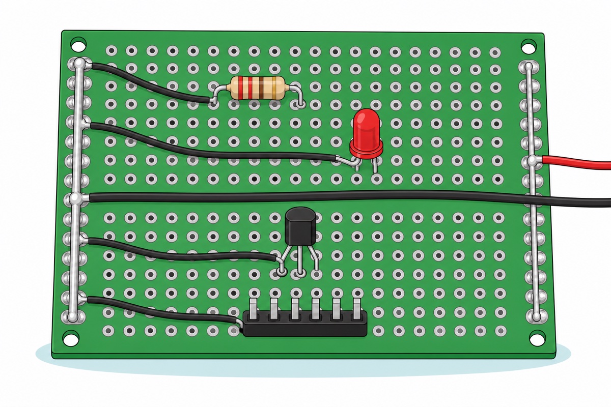
A rail is a bare wire lying along one row of pads, soldered at every pad it crosses. A cut-off resistor or LED leg is ideal stock — stiff, pre-tinned, free — and the column of elongated oval pads down each edge is its natural home, an oval giving more copper to solder to than a round ring. Ground down one edge, 5 V or 3.3 V down the other. Either face will do — the solder side is usually the clearer one — and the wire wants tacking at both ends first, pulled straight, before you solder the pads in between; a rail worked pad by pad from one end wanders off the row.
A rail is one node along its whole length, so every point on it is electrically the same place: a component’s ground only has to reach the nearest point on the rail instead of chasing back to the microcontroller, and one wire then carries the lot from rail to GND pin. When a part sits too far from the edge to reach comfortably, solder a second offcut out of the rail and into the middle of the board — a spur off one node is still that node.
The copper itself is free: seventy millimetres of 0.6 mm component leg is about four milliohms, so half an amp down the whole rail drops two millivolts. Topology is what costs. Daisy-chained grounds put every joint inside the return path of everything downstream, so one cold joint takes out several parts at once. A ground landing straight on the rail fails alone, and is far easier to find.
One honest limit: a shared rail carries every load’s return current, and the millivolts it drops move the reference under anything measuring against it. Give a motor or relay coil its own wires back to the supply, not the rail your analogue parts sit on.
What are the three honest ways to join two pads?
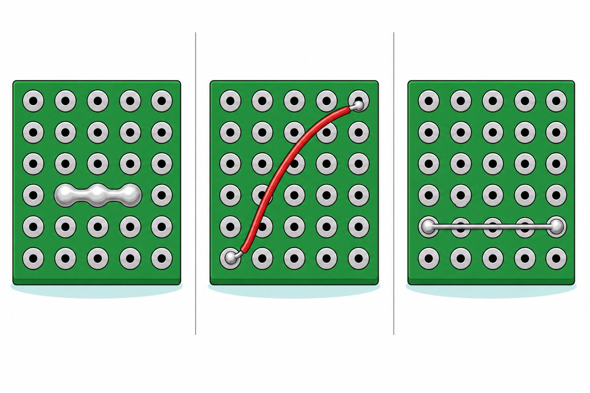
A solder bridge — sambung tapak — is molten solder spanning the green solder mask between two neighbouring rings. Solder wets clean, hot copper and will not wet the mask at all, so the bead is held only by the two pads at its ends and by its own surface tension: on a 2.54 mm pitch with a pad ring just under 2 mm, that unsupported span is a little over half a millimetre, which surface tension carries easily. The same physics predicts both failures — a pad cooler than the solder, or oxidised with its flux boiled off, is never wetted, so the solder balls up on the hot pad alone; and every pad you add lengthens a bead whose middle rests on mask it cannot grip, until it thins, cracks and opens. Two to four pads is technique. Past that, lay a bare leg offcut instead.
An insulated wire jumper on the component side handles any distance and crosses other connections without touching them. Strip about 5 mm from a jumper wire — cut the moulded pin off, the flexible wire inside is the useful part (see our jumper wire guide) — then twist and tin the end so it feeds through a 1 mm hole instead of fraying.
A component-leg offcut sits between the two. Snipped resistor and LED legs are stiff, pre-tinned solid copper: bend one flat along the solder side, drop its ends into two pads a few holes apart, and it stays put while you solder. Keep the offcuts — the wire you use most.
| Method | Reaches | Use it when | Fails as |
|---|---|---|---|
| Solder bridge | 1–3 pads | Joining pads that are already neighbours | A sagging chain, or a bridge you did not intend |
| Bare leg offcut | 2–10 pads, straight lines | Rails, and short hops on the solder side | A short where it crosses another bare run |
| Insulated wire | Any distance | Crossing the board, or over other connections | Strands fraying out of the hole onto a neighbour |
Of the three, the bridge is the one with a knack, and the knack is temperature rather than quantity of solder. Set the iron around 300–350 °C — leaded solder melts near 183 °C and both pads have to climb well past that before either will take it — then lay the tip so it touches both rings at once, feed a little solder into the corner where tip meets copper, and let the pool spread across the gap by itself before lifting off. Feeding solder onto the tip instead of into the joint is what leaves a ball sitting on one pad; a pad that still refuses usually wants a dab of rosin paste, not more solder.
The wrist movement behind a dragged bridge:
How do you plan the layout before the iron is hot?
Capture the circuit before you take it apart. The working breadboard is the only copy of the design you own, and pulling the first wire erases it: photograph it from directly overhead, then write the connections out as plain lines — “sensor OUT to ESP32 GPIO 4”, “every ground to the ground rail” — one line per connection. You then solder from that list, not from memory of a board that no longer exists.
The donut board punishes improvisation: unsoldering is far slower than soldering. Draw it first on squared paper, one square per pad, using the row letters printed up the board’s edge as coordinates, so “resistor H7 to H10” still means something next week.
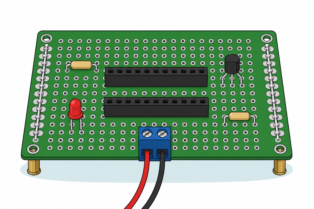
Connectors, power input and anything with a cable belong at the board edge, so wires leave without crossing the middle. Give the microcontroller a female header socket rather than soldering it down — a socketed board survives a mistake in the rest of the circuit, comes out for reflashing, and moves to the next project. Align it the easy way: push both socket strips onto the module’s own pins first, lower the whole assembly into the board, solder one end pin of each strip, check the module still sits flat, then solder the rest. Two loose strips aligned by eye is how a board ends up with a socket the module will not go into. Keep the four corner holes clear for standoffs.
The mirror catches everyone once. Flip the board to solder and left and right swap, because you now read the same grid from behind — a chip positioned by counting pads from the left edge on the solder side lands mirrored. Mark one corner on both faces and count from that dot.
Work in order: rails, sockets and headers while the board lies flat, then low parts, tall or heat-shy last. Two checks before power. Look along the solder side at a shallow angle under a lamp — unintended bridges show as a silver ridge where there should be green. Then beep, with a multimeter on continuity: rail to every ground leg, and supply against ground, which must not beep.
The whole move, start to finish:
Common mistakes we see from real customers
Expecting the five-hole row to still be there. The commonest failure is a layout copied hole-for-hole from the breadboard, two legs in adjacent pads with nothing joining them: identical to the working build, and electrically open.
Stacking every ground onto one pin. The instinct is the customer’s own: “kite sambung wayar komponen ground tuh dekat expansion board esp32 tuh kan” — run every component’s ground wire to the board’s GND pin. Right destination, wrong route. Four or five wires will not go into one hole, twisting them together outside it makes a joint nobody can inspect, and one loose twist opens the return path for everything at once. Land them on the rail; the rail keeps the single wire to GND.
Bridges nobody meant to make. Too much solder, or an iron parked on one spot until the flux burns away, spreads a blob onto a neighbour — usually under a header where you cannot see it. Angled light finds them; the desoldering pump removes them.
Cold joints that pass a visual check. Where only the solder melted and not the pad, it sits on the ring as a dull grey ball instead of a shiny cone — fine on the bench, open once the board moves. Reheat until it flows, adding fresh flux-cored solder.
Trimming legs before soldering. A leg cut flush first has nothing holding it while the solder cools, so it lifts as the board is turned. Push each leg fully through and splay it flat against the copper side at roughly forty-five degrees — that alone clamps the part while you flip the board over. Solder long, then flush-cut with the Plato 170 cutter — its 1 mm rating covers component legs, not steel or mains wire.
Pulling a pad off the board. The ring is thin copper foil bonded to fibreglass, and that bond is the weakest thing on the board: rest the iron on one pad while you hunt for the solder and the adhesive lets go, or tug a power cable once and the ring leaves with it. In and out in a second or two, and give every cable that leaves the board a strain relief — thread it down through a spare hole, back up through the next one, and solder it only after that loop, so a pull lands on fibreglass instead of on the joint.
FAQ
What is a donut board and how is it different from a breadboard?
A donut board is a fibreglass PCB on a 2.54 mm grid with an isolated copper ring around every hole — perfboard and prototype PCB are other names for it. A breadboard joins five holes per row behind a hidden clip; a donut board joins nothing, so you solder every connection.
How do I connect two pads on a donut board?
Three ways, by distance. Neighbours: a solder bridge across the sub-millimetre gap between two rings, heating both pads or it sticks to only one. A few pads apart: a bare component-leg offcut soldered flat on the solder side. Further, or crossing others: an insulated wire, stripped and tinned.
Do I need to cut any copper tracks on a donut board?
No. That is stripboard or Veroboard, whose copper strips need a track cutter where a connection is unwanted. A donut board’s pads are isolated already, so there is nothing to cut, and no unwanted connection except one you solder by accident.
Why did my circuit stop working after I soldered it to the donut board?
Almost always one of three: two legs in adjacent pads with nothing joining them now the hidden row is gone; a cold joint that conducts on the bench and opens when the board flexes; or an unintended bridge shorting a signal to its neighbour. Beep supply against ground on continuity first, then every connection you meant to make.
Should I solder my ESP32 or Arduino straight onto the donut board?
Better not. Solder a female header socket into the donut board and plug the module into it. A soldered-down module cannot be swapped when it dies, cannot move to the next project, and has to survive every heat cycle of the build, while a socketed one lifts out in a second. Push the sockets onto the module’s own pins before soldering them, so the spacing cannot drift.
Last updated August 2026. Stuck? Chat with us on WhatsApp.
