

Tutorials
TP4056 How to Use: Charge an 18650 Safely + Boost to 5V
Aug
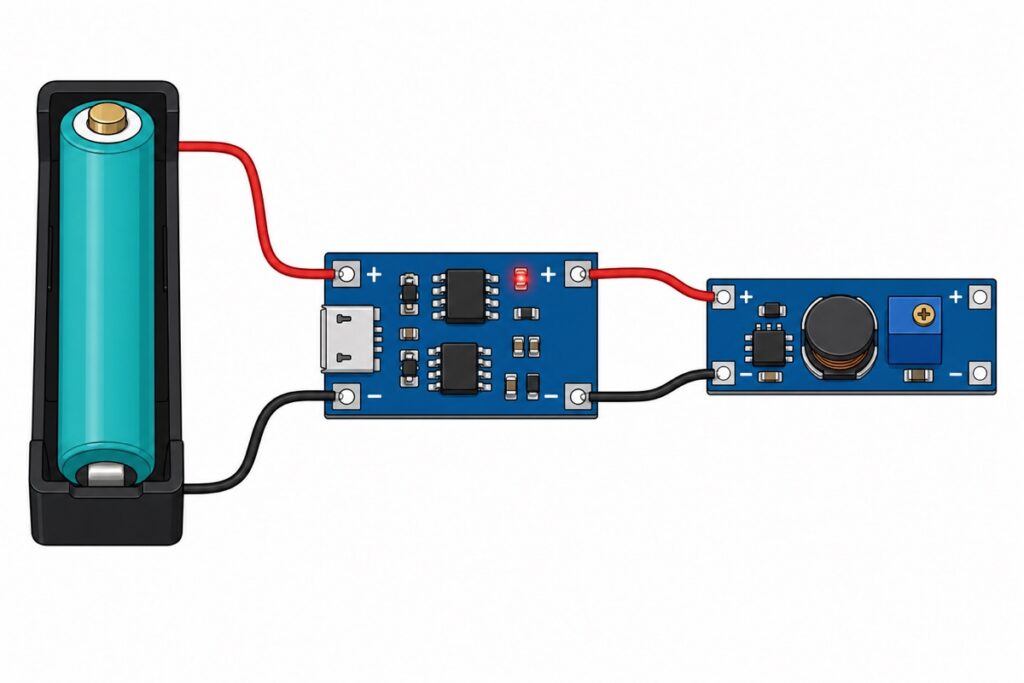
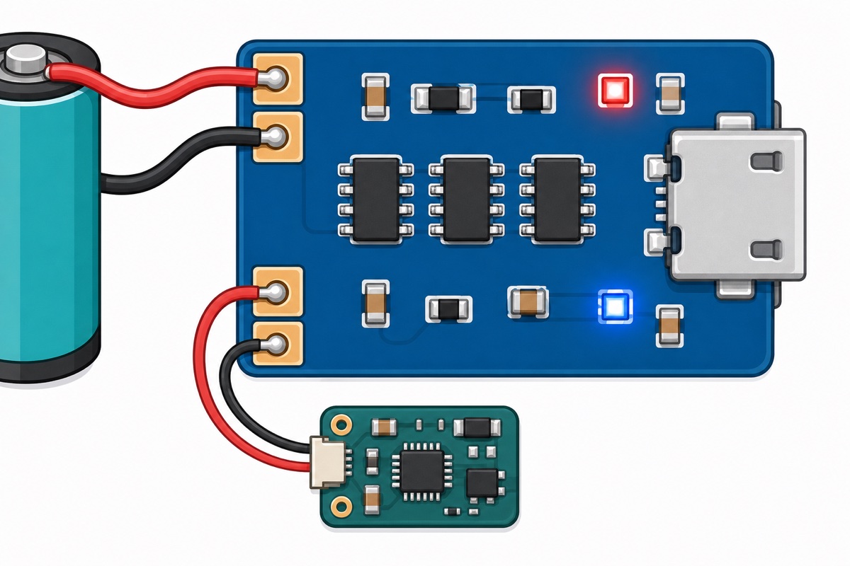
To charge an 18650 safely with a TP4056, connect the cell to B+ and B− and your project to OUT+ and OUT− — never to the battery pads. The protection MOSFETs sit between B− and OUT−, so a load there bypasses them. The board charges to a fixed 4.2V, and an MT3608 boost converter turns that into a steady 5V.
What do the TP4056’s B+, B−, OUT+ and OUT− pads actually do?
The TP4056 modules in this guide are the protected version, which is why they carry four pads rather than two: B+ and B− for the cell, OUT+ and OUT− for your project. The two pairs are not interchangeable, even though a multimeter reads almost the same voltage on both.
A protected board adds two more chips: a controller, typically a DW01A, plus the dual MOSFET pair it switches. Both FETs sit in the negative rail, as the application circuit in the DW01A datasheet shows. B+ and OUT+ are therefore the same electrical node, and the switching all happens between B− and OUT−.
A load soldered to B+ and B− therefore taps the cell before those MOSFETs. Everything still appears to work — the board charges, the project runs, the LEDs behave — but over-discharge, over-current and short-circuit protection are all no longer in the path.
Parts list
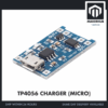 TP4056 18650 Battery Charger Module Lithium Ion Battery Li-ion Battery Charger Type C Micro USB - TP4056 CHARGER (MICRO)
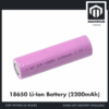 3.7V 18650 Battery Rechargeable Li-Ion Battery 1200mAh 2200mAh 3200mAh Flat Top - 18650 Li-Ion Battery (2200mAh)
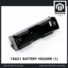 18650 Battery Holder 1/2/3/4 Slot 3.7V Battery Cell Housing Battery Case Battery Casing - 18650 BATTERY HOLDER (1)
 MT3608 Adjustable Step-up Convertor Boost Converter Switching Boost Converter for Arduino Project
| Board pad | Connects to | Why |
|---|---|---|
| B+ | 18650 positive (holder’s red wire) | Goes to the charger IC’s BAT pin — this is the cell node |
| B− | 18650 negative (holder’s black wire) | Sits on the battery side of the protection MOSFETs |
| OUT+ | Your project’s + rail, or the MT3608’s VIN+ | Same net as B+; the plus side is not what gets switched |
| OUT− | Your project’s ground, or the MT3608’s VIN− | The protected node — every milliamp here passes through the MOSFET pair |
| USB socket / IN pads | A 5V phone charger | The datasheet rates supply voltage 4.0V to 8.0V, 5V typical |
Prefer to see the board on real hardware? This walkthrough is a good companion:
How do I tell a protected TP4056 from a bare one?
A protected TP4056 board is easiest to identify by counting chips: three beside the pads — the TP4056 itself plus two 6-pin SOT-23 parts, typically a DW01A and an FS8205A. A bare board carries the TP4056 alone and has no OUT pair.
| Feature | TP4056M | TP4056C | Bare TP4056 board |
|---|---|---|---|
| Input connector | Micro-USB | USB Type-C | Either |
| Protection circuit | Yes | Yes | No |
| Chips beside the TP4056 | Two SOT-23-6 | Two SOT-23-6 | None |
| Silkscreen at the pads | A B+/B− pair and an OUT+/OUT− pair | A B+/B− pair and an OUT+/OUT− pair | No OUT pair |
| Over-discharge cut-off | Yes | Yes | No |
| Charge current as supplied | 1A | 1A | 1A |
How do I change the TP4056’s charge current?
The TP4056 sets charge current with one resistor from PROG to ground — usually the part marked R3. Its datasheet gives IBAT = (VPROG ÷ RPROG) × 1200 with VPROG = 1V, and also prints a lookup table that disagrees with it slightly. Where they differ, follow the table.
Battery University advises charging at 0.5C to 1C. For the 2200mAh cell here, the stock 1A works out at 0.45C, so leave it alone. Small LiPo pouches are the ones that suffer: 1A into a 500mAh pouch is 2C.
| R3 (RPROG) | Charge current | Suits a cell of roughly |
|---|---|---|
| 1.2 kΩ (as supplied) | 1000 mA | 2000 mAh and up |
| 2 kΩ | 580 mA | 1200 mAh |
| 3 kΩ | 400 mA | 800 mAh |
| 5 kΩ | 250 mA | 500 mAh |
| 10 kΩ | 130 mA | 260 mAh |
What do the TP4056’s red and blue LEDs mean?
The TP4056 drives its LEDs from CHRG and STDBY, both open-drain outputs that can only pull down or float. Red (CHRG) means the cell is charging; blue or green (STDBY) means charging has finished.
The behaviour that confuses people is the no-cell case. With nothing on the battery pads the datasheet says both LEDs stay off, but add a little capacitance across BAT, such as a 10µF capacitor or an empty holder’s leads, and the standby LED lights while the charge LED blinks on a one-to-four-second period. That is documented, not a fault.
When does the TP4056 stop charging, and what does the protection cut off?
The TP4056’s float voltage is fixed at 4.2V — specified 4.137V minimum, 4.2V typical, 4.263V maximum. It runs constant current up to that point, holds 4.2V while the current tapers, then terminates at a tenth of the programmed current. A Li-ion cell cannot absorb a trickle, so charging has to stop.
The protection circuit is a separate, later line of defence. Its DW01A thresholds sit well outside normal use, so in a healthy build you should never reach them.
| Event | Trip point | Recovers at |
|---|---|---|
| Over-charge | 4.30V typical (4.25–4.35V) | 4.10V typical |
| Over-discharge | 2.40V typical (2.30–2.50V) | 3.00V typical |
| Over-current | 150mV across the MOSFET pair | Load removed |
| Short circuit | 1.2V across the MOSFET pair, 5µs | Load removed |
Over-current is specified as a voltage rather than an amperage: the trip current is 150mV divided by the on-resistance of the MOSFET pair, and that resistance varies between batches. Treat it as a backstop and fuse the circuit properly instead.
How do I boost 3.7V to 5V with the MT3608?
The MT3608 boost converter turns a sagging cell into a steady 5V rail, which matters because a “3.7V” 18650 is 4.2V when full and about 3.0V when nearly flat. Wire OUT+ and OUT− to the module’s VIN+ and VIN−, then take 5V from VOUT+ and VOUT−.
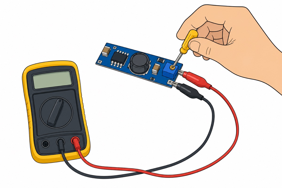
Setting the output voltage is the step most people rush. Power it up, put your meter on VOUT+ and VOUT− while it is running, then turn the small blue trimmer slowly — it is a multi-turn part, so one volt takes many turns. Our digital multimeter guide covers the settings, and the opposite job is in our LM2596 buck converter guide.
Next comes the current budget, where a boost converter surprises people: it moves power, not current. 5V at 0.5A is 2.5W out, which at a realistic 85% efficiency needs 2.94W in — 795mA from a 3.7V cell, and 980mA from a nearly empty 3.0V one.
That is also why a boost module’s “2A” deserves a second look. The MT3608 datasheet specifies a 4A internal switch current limit, and that is input-side current, so the further you step the voltage up, the less reaches the output. The datasheet’s own figures are 2V–24V in and up to 28V out; module listings often quote something narrower. Trust the datasheet and that 4A switch limit over any headline number.
Can I charge the 18650 and run my project at the same time?
The TP4056 has no power-path management, and that single fact is the whole answer. A charger with power-path runs your load from the input supply while charging the cell separately; the TP4056 has only one battery node, so load and cell share it.
Leave a load on OUT+ and OUT− while charging and the current the chip regulates is no longer only what enters the cell. Because termination waits for that current to fall to a tenth of the programmed value, a load above a tenth of the programmed charge current — 100mA at the stock 1A setting — can stop the board ever finishing. Charge the cell first, then run the project.
What are the real safety rules for a single-cell 18650 build?
An 18650 stores real energy, so a few habits are worth keeping. Do not solder to a bare cell body with an ordinary iron, because the heat travels inside — use a holder or spot-welded tabs. Do not charge a cell unattended overnight on a breadboard, where one nudged jumper is a dead short. And pairing an already-protected cell with a protection board is not dangerous, just redundant — whichever cut-off trips first takes the pack down, and a cell whose own board has latched off at its cut-off can be awkward to revive. One layer is enough.
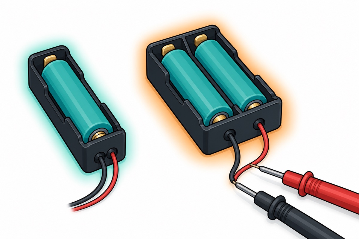
The mistake that catches builders most often is the battery holder. Multi-slot 18650 holders are sold both ways — series (two slots give 7.4V, three give 11.1V) and parallel (still 3.7V, just more capacity) — and the casing almost never says which. The TP4056 charges exactly one cell to 4.2V, so anything above that is wrong. Measure the holder’s leads first: near 3.7V means single or parallel, near 7.4V means series. For 1S, use a single-slot holder.
What if I just want a ready-made USB power bank?
The 37VUSBD dual-USB power bank board suits the reader who would rather not build a circuit at all: charger, boost converter, protection and a battery-percentage display on one PCB, with a 5V USB output. What you typically give up is control — no changing the charge current, no output but 5V, no raw-cell tap for 3.3V logic.
Optional but worth it
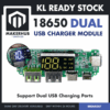 18650 Battery Charger Boost Module Dual USD Output Charging Module 5V with Charging Protection
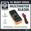 XL830L Digital Multimeter with backlight Portable Multimeter Electronics Project
How do I read the battery voltage from an ESP32?
An ESP32 cannot read 4.2V directly, because its GPIOs run at 3.3V, so a voltage divider is not optional. Two 100kΩ resistors from OUT+ to ground, with the ADC on the junction, halve it: a full cell arrives at the pin as 2.10V. The divider bleeds 4.2 ÷ 200,000 = 21µA, negligible against a 2200mAh cell.
It is worth being honest about what the ADC hands back. Espressif’s calibration docs note that the nominal 1100mV reference varies from 1000mV to 1200mV between chips, and that the ADC is noise-sensitive. That is why the sketch below uses analogReadMilliVolts(), which applies your own chip’s burned-in calibration.
// 18650 pack voltage and rough percentage - ESP32
// Divider: OUT+ --[100k]--+--[100k]-- GND, ADC on the junction (GPIO34).
// A full 4.2 V cell arrives at the pin as 2.10 V, well under the 3.3 V rail.
// Divider drain: 4.2 / 200000 = 21 uA. Negligible against 2200 mAh.

const int   VBAT_PIN = 34;    // input-only ADC1 pin - keeps working with WiFi on
const float DIVIDER  = 2.0;   // 100k + 100k = divide by two
const int   SAMPLES  = 32;    // the ESP32 ADC is noisy; average it

void setup() {
  Serial.begin(115200);
  analogSetPinAttenuation(VBAT_PIN, ADC_11db);   // widest attenuation
}

// APPROXIMATE Li-ion curve - a rough guide, not a fuel gauge.
// Real capacity depends on load, temperature and cell age.
float percentFromVolts(float v) {
  const float pts[][2] = {
    {4.20, 100}, {4.00, 80}, {3.85, 55}, {3.70, 30}, {3.50, 10}, {3.00, 0}
  };
  const int n = 6;
  if (v >= pts[0][0]) return 100.0;
  for (int i = 1; i < n; i++) {
    if (v >= pts[i][0]) {
      float span = pts[i - 1][0] - pts[i][0];
      float frac = (v - pts[i][0]) / span;
      return pts[i][1] + frac * (pts[i - 1][1] - pts[i][1]);
    }
  }
  return 0.0;                  // below 3.00 V - the protection is about to cut in
}

void loop() {
  uint32_t mv = 0;
  for (int i = 0; i < SAMPLES; i++) {
    mv += analogReadMilliVolts(VBAT_PIN);   // uses this chip's eFuse calibration
  }
  float packV = (mv / (float)SAMPLES) * DIVIDER / 1000.0;

  Serial.print(packV, 2);
  Serial.print(" V  ~");
  Serial.print(percentFromVolts(packV), 0);
  Serial.println(" %");

  delay(2000);
}
Take the reading while the project is idle, because cell voltage sags under load. If the board will not connect at all, see our guide on fixing an ESP32 that is not detected.
Common mistakes we see from real customers
The TP4056 is unusually easy to wire in a way that looks perfectly fine and is quietly wrong. Five failure modes keep coming back.
The most common one is a load soldered to B+ and B−. It is the shorter route on a crowded board and it works, so nothing prompts a second look — but the protection MOSFETs sit between B− and OUT−, which leaves that load outside them. The cell can then be pulled below 2.4V, and a cell taken that low rarely recovers.
Second is the multi-slot holder: two cells in series present 7.4V to a chip that assumes one. Third is adjusting the boost converter only after the project is connected, because at many turns per volt 5V is easy to overshoot, and the project pays for it.
Fourth is a module that looks dead with no cell in the holder, which is documented behaviour rather than a fault. Fifth is reading a boost module’s “2A” as a guarantee at the output.
FAQ
Can I use a TP4056 for 3 batteries?
Only if the three cells are wired in parallel, and only with cells of the same make, capacity and state of charge — wiring a full cell to a flat one dumps a large current between them, so measure both first and match them to within about 0.05V. A parallel pack is then still one 3.7V cell with triple the capacity. Three cells in series is 11.1V, and the TP4056’s input pin tops out at 8V absolute maximum, so that destroys the module.
Why is my TP4056 hot?
The TP4056 is a linear charger, so every volt it drops becomes heat — about 1.4W at 1A with 5V in and a 3.6V cell. Warm is normal. If it is too hot to touch comfortably, fit a larger R3 so it charges at a lower current.
How long does it take to charge an 18650?
At the stock 1A into a 2200mAh cell, budget about three hours: roughly two hours at constant current, then a taper until the current falls to a tenth of 1A.
Can I leave it charging overnight?
Electrically it stops on its own, because it terminates at C/10 and does not trickle-charge afterwards. The risk is the setup around it: a breadboard, loose jumpers, a cell that can shift. Charge somewhere you can see it.
TP4056 no light when I plug in?
Check the cell first. With no battery attached the datasheet says both LEDs stay off, so a dark board usually means the holder is not gripping the cell properly. The datasheet gives the same both-off state when the input voltage is too low, so try another cable and charger before blaming the board.
Last updated August 2026. Stuck? Chat with us on WhatsApp.

Pingback: Lithium Battery Types: Li-ion vs LiPo vs LiFePO4
Pingback: NiMH vs Alkaline AA: 1.2V or 1.5V for Your Project
Pingback: Remote Control Car RBT Project: 3 Ways to Build It